Emerging Technology48 min read
PoppyUp: Rugged Camera Card Offload Device
By Richard Pruitt ·
Source code: PoppyUp · 88 files · browse and download (7.3 MB zip)
I have spent a long time thinking about a small, specific problem: getting footage off a camera card and into a safe place, fast, without a laptop, and without ever putting the card at risk. The result is a complete Phase 1 hardware design package for a device I call PoppyUp. It has an architecture decision record, requirements with acceptance criteria, a system block diagram, a data-path analysis, component selection with part numbers, a power budget, a thermal plan, an RF plan, a mechanical concept with drawings, a PCB architecture, a bill of materials at 1,000 and 10,000 units, a certification plan, a ranked risk register, a prototype roadmap, a ten-sheet wiring diagram set, and an interactive 3D assembly viewer.
I am not going to build it. I don't have the time, and a hardware program of this size needs a team and a few million dollars. Rather than let the work sit on a disk, I'm publishing all of it for free. This post is the long-form tour: why a tool like this is worth building, how the device works in detail, how it is configured, what it costs, and exactly what you would do, stage by stage, if you picked the package up tomorrow.
Everything below comes from the package as it stands at ADR baseline v0.3 (2026-09-27). Where a number is a model prediction rather than a measurement, the package marks it "verify" and I keep that marking here. No firmware or app code exists yet; that is Phase 2 and Phase 3, by design.
Part 1: Why this tool is worth building#
The problem#
A professional camera card is often the only copy of a day's work. Between the moment the camera stops recording and the moment the files land on a second drive, every bump, every mis-click, every laptop crash is a risk to something that cannot be re-shot. Digital imaging technicians (DITs), event shooters, documentary crews, wedding photographers and sports entertainment teams all live with this gap. The standard answer is a laptop, a card reader, offload software and a lot of discipline.
That workflow has four persistent weaknesses:
It needs a laptop. A laptop on a venue table, in a vehicle, on a hotel desk, with a reader dangling off it, is a fragile, power-hungry and theft-prone way to copy files.
Operating systems write to cards. macOS silently creates
.Spotlight-V100,.fseventsd,.Trashesand._*files on any writable volume within seconds of mounting it. Windows updates access times. A card that has been "just mounted" is no longer byte-identical to what came out of the camera, and some cameras object.Copies are not verified by default. Finder and Explorer copy; they don't checksum. Verification is an extra step that gets skipped under time pressure.
"Fast" is relative. A CFexpress Type B card reads at 3.5 GB/s. A hotel's internet uplink moves 5 MB/s. The honest bottleneck in the field is almost never the hardware you bought; it's the network you happen to be standing next to.
What PoppyUp does about it#
PoppyUp is a battery-powered, ruggedized brick (190 × 96 × 38 mm, about 828 g) with five card slots along its top edge under a sliding metal shutter. You insert a card, and the device:
mounts it read-only, never writes to it, never "repairs" it, never clears a dirty bit;
streams the files directly to SFTP, S3-compatible storage (Amazon S3, Backblaze B2, Wasabi, Cloudflare R2), Google Drive or Dropbox, with no mandatory intermediate copy;
checksums every object end to end, with per-chunk hashing while streaming and remote verification through each endpoint's native mechanism;
resumes across link loss, power loss, reboot, card removal and mode switches, re-sending at most one in-flight chunk;
picks the best available link automatically, in the order Ethernet, then Wi-Fi, then a USB-tethered phone, with metered-link caps and warnings;
writes a manifest per job, including the phone's location if the app supplies it.
Plugged into a Mac, PC, iPad or iPhone, it becomes a driverless card reader that presents the cards read-only by default. On the Pro model, a third port hands the CFexpress B card straight through to the host at USB4 speed (about 3 GB/s), which is what a professional expects from a modern reader.
The design is deliberately honest about the network. The internal card path runs at 1.65 GB/s. The best wired network it can attach to, 5GBASE-T, drains at about 500 MB/s. A typical venue drop is 10 to 120 MB/s. A phone's real-world 5G uplink is 2.5 to 25 MB/s. PoppyUp is built so that it is never the bottleneck; whatever network you have is. That one sentence shaped most of the decisions in the package, including the decision to drop the built-in cellular modem (more on that in Part 7).
Who it is for#
DITs and data wranglers on a cart in a studio or venue with a wired drop: a 512 GB card uploads to S3 in about 17 minutes over 5GbE and the device is back in the shooter's hand after a quick copy in under 3 minutes (Pro model).
Event and documentary shooters working from a hotel room or a car: the device uploads in the background over Wi-Fi or the phone they already carry, charging that phone while it works.
Anyone who wants a card reader that cannot modify their media. Even the reader mode is read-only by default on both USB paths.
Where it sits in the market#
The package positions it as a "pro accessory" at a BOM-implied retail band of roughly $1,200 to $1,550 for the Base model at launch volumes, falling toward $800 to $1,050 at 10,000 units per year. Reference points from the BOM document: a USB4 CFexpress 4.0 reader is $80 to $150; Gnarbox-class field backup devices sold for $500 to $900; a broadcast bonded-cellular encoder is $3,000 to $8,000. The price will be judged against hiring a DIT with a laptop, not against consumer readers. The target retail price and program budget ceiling are explicitly not set in the package; that is one of the open decisions.
Part 2: The device at a glance#
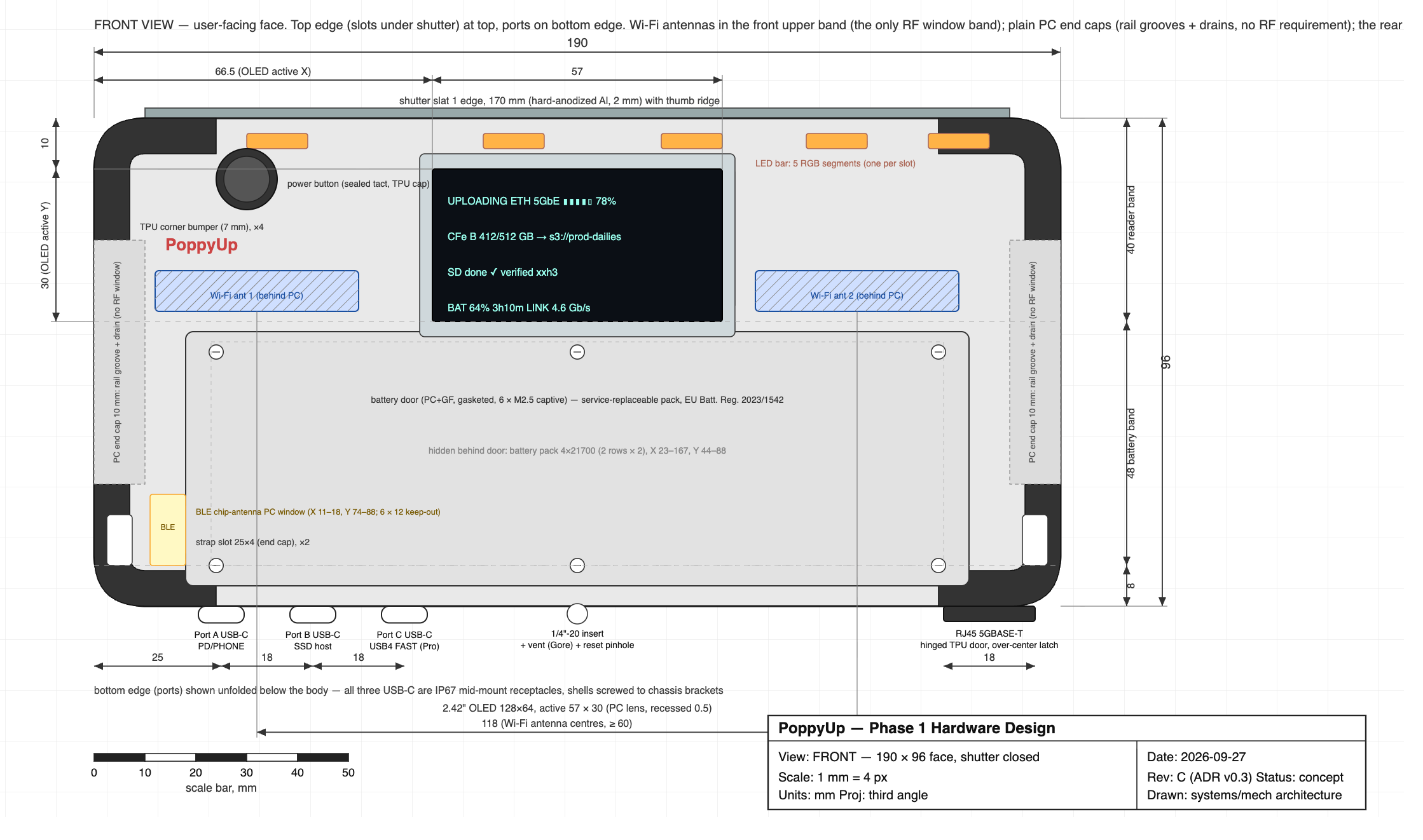
| Item | Specification |
|---|---|
| Size and mass | 190 × 96 × 38 mm, about 828 g (magnesium chassis) |
| Media slots (top edge, left to right) | CFast 2.0, CFexpress Type B, CFexpress Type A, SD UHS-II, microSD |
| Shutter | Two-slat sliding hard-anodized 6061 aluminum, POM tracks, magnetic closed-detect |
| Ruggedness | MIL-STD-810H Method 516.8 Proc. IV drop, 1.22 m onto concrete, 26 drops; IP54 shutter closed, IP52 open |
| Compute | Rockchip RK3588 (industrial RK3588J preferred), 8 GB LPDDR4x, 64 GB eMMC, TPM 2.0 |
| Embedded controller | Nordic nRF5340, always on, owns power, thermal, display, mode switching and BLE 5.4 |
| Network | 5GBASE-T Ethernet (Realtek RTL8126), Wi-Fi 7 2×2 (MediaTek MT7925), BLE 5.4; no built-in cellular |
| Ports (bottom edge) | Port A USB-C "PD / PHONE" (charge, reader, management); Port B USB-C "SSD / TETHER" (10 Gbps host, 5 V source); Port C USB-C "USB4 / CFexpress FAST" (Pro only); RJ45 behind a door |
| Battery | 4 × 21700 Li-ion, 2S2P, 72 Wh; USB-C PD 3.1 sink up to 65 W; 0→80 % in about 1.6 h |
| Runtime | 4.4 h continuous 5GbE upload, 6 to 8 h on Wi-Fi or hotspot, about 3 weeks standby |
| Display | 2.42" 128 × 64 monochrome OLED driven by the EC; 5-segment RGB LED bar |
| Operating temperature | −10 to +40 °C full performance, −20 to +50 °C with throttling; charge 0 to 45 °C |
| SKUs | Base; Pro adds the USB4 pass-through port, a Port C power input and a 1 TB internal NVMe. Same PCBs, same enclosure |
The design is a sealed, passively cooled box. Every design choice downstream of that fact, from the magnesium chassis to the 5GbE rather than 10GbE Ethernet, exists to make about 10 W of continuous heat and a 15-minute 15 W burst survivable without a fan.
Part 3: How it works, subsystem by subsystem#
3.1 The big idea: everything is a PCIe endpoint#
PoppyUp is a PCIe-centric design. Every card slot, the Ethernet controller, the Wi-Fi module, the optional NVMe and the USB host controller are PCIe endpoints hanging off an RK3588 root complex. The RK3588 was chosen because it is the only sub-$50 application processor that offers four PCIe Gen3 lanes split across two controllers, three more Gen2 lanes, and two genuinely dual-role USB 3 controllers with mature gadget support in mainline Linux. Its four Cortex-A76 cores with crypto extensions sustain TLS plus SHA-256 plus xxHash at 5GbE rates on about 1.5 cores.
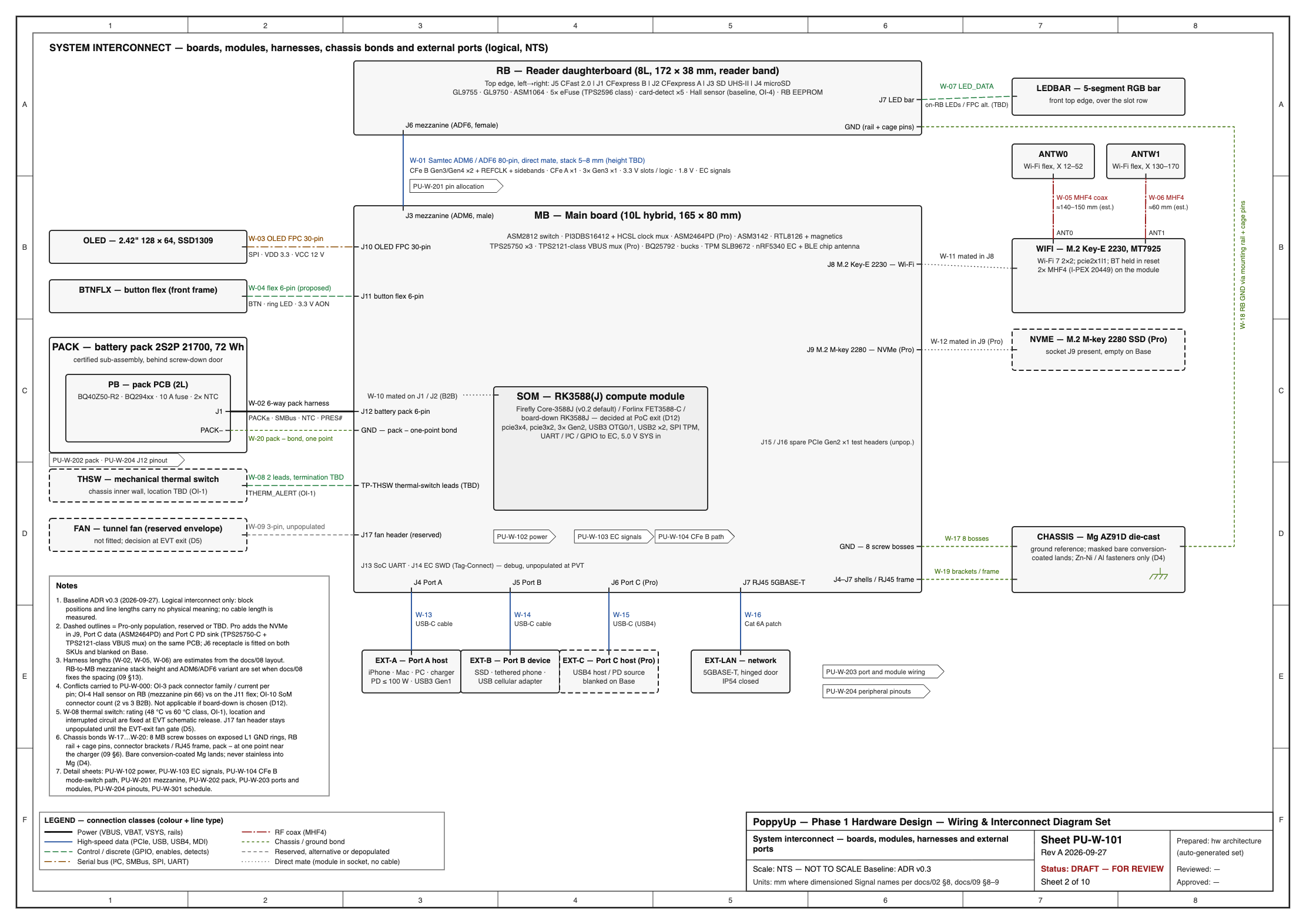
The lane map:
| RK3588 port | Width | Goes to | Why |
|---|---|---|---|
pcie3x4, bifurcated to Gen3 ×2 | 2 lanes | CFexpress Type B slot through a Diodes PI3DBS16412 Gen4-rated 2:1 mux | The top-priority slot gets its own root port so it never competes, and so it can be handed cleanly to the USB4 bridge |
pcie3x2, Gen3 ×2 | 2 lanes | ASMedia ASM2812 packet switch (×2 up, 12 lanes down) | Everything else |
| ASM2812 downstream ×1 | CFexpress Type A slot | The card is itself an NVMe device | |
| ASM2812 downstream ×2 | M.2 2280 NVMe (Pro; socket empty on Base) | Buffer and quick-copy at ~1.6 GB/s | |
| ASM2812 downstream ×1 | Realtek RTL8126 5GbE | RK3588's native MACs are 1 GbE only | |
| ASM2812 downstream ×1 | Genesys GL9755 SD UHS-II host | RK3588's native SD host is UHS-I only | |
| ASM2812 downstream ×1 | Genesys GL9750 microSD host | Keeps microSD on the same fabric | |
| ASM2812 downstream ×1 | ASMedia ASM1064 AHCI SATA → CFast 2.0 | CFast is SATA III | |
| ASM2812 downstream ×2 | ASMedia ASM3142 xHCI → Port B (USB 3.2 Gen2, 10 Gbps) | External SSD ingest at ~900 MB/s; also the host for tethered phones | |
pcie2x1l1, Gen2 ×1 | 1 lane | M.2 Key-E 2230 Wi-Fi 7 module | A 2×2 Wi-Fi 7 client moves 1.5 to 2.5 Gb/s, under a Gen2 lane's ~3.2 Gb/s |
pcie2x1l0, pcie2x1l2 | 2 lanes | Spare, on internal test headers | Future daughterboard attach points |
Nine of the switch's twelve downstream lanes are used. Nothing is oversubscribed at the root: the aggregate of realistic concurrent flows fits because the CFexpress B slot shares its port with nothing.
The USB side:
| Controller | Role | Port |
|---|---|---|
| RK3588 USB3 OTG1 (dwc3, 5 Gbps) | Device (gadget): one UAS/BOT mass-storage LUN per card plus a CDC-NCM management network | Port A |
| ASM3142 (10 Gbps) | Host: external SSD, USB-tethered phone, USB cellular adapter | Port B |
| ASMedia ASM2464PD (USB4 40 Gbps ↔ PCIe Gen4 ×4 bridge, falls back to USB 3.2 Gen2 UAS) | Device: CFexpress B pass-through | Port C (Pro only) |
3.2 The card slots and the reader daughterboard#
The five slots sit in a 6 mm deep, 22 mm wide channel along the top edge. Order, left to right from the front: CFast | CFexpress B | CFexpress A | SD | microSD. The two thick, hot cards sit at the left, away from the Ethernet PHY; CFexpress B is second from the left so a thumb lands on the most-used slot; the thin SD cards sit by the OLED so icons and status read together.
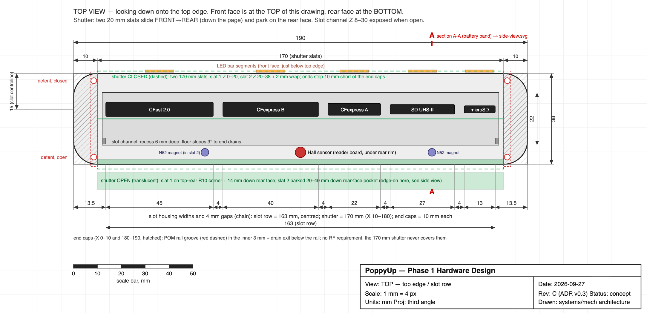
All connectors are deep-insertion push-push types so a seated card sits at least 1 mm below the shutter plane. Each slot has its own eFuse with a current limit, a card-detect line to the EC (which also wakes the device from standby), and the CFexpress B and CFast cages are thermally bridged to the chassis so card heat does not stay in the reader band.
The reader function lives on an internal 8-layer daughterboard (about 172 × 38 mm) joined to the main board by an 80-pin Samtec ADM6/ADF6 0.635 mm mezzanine carrying CFexpress B Gen3 ×2 plus reference clock, CFexpress A Gen3 ×1, three more Gen3 ×1 lanes for the SD, microSD and SATA controllers, reset and clock-request sidebands, I²C, card-detect and at least 6 A of 3.3 V. The point is that a no-CFast variant, a dual-CFexpress-B variant or a future SD Express variant is a daughterboard swap, not a main-board re-spin.
Two notes on what is deliberately not supported. XQD cards fit physically in the CFexpress B slot but use a proprietary non-NVMe PCIe protocol with no Linux driver; the only XQD behaviour in the product is detecting a non-NVMe device and showing "XQD not supported". SD Express and UHS-III host modes are also out: UHS-III has no cards, SD Express has negligible camera adoption, and SD Express cards fall back to UHS-I in this slot. A footprint-compatible GL9767 upgrade path exists if the market appears.
3.3 Standalone mode: the upload engine's hardware contract#
In standalone mode every slot mounts read-only and the job engine streams file → chunk → hash → TLS → endpoint with no intermediate copy. The hardware promises three things to the firmware:
Throughput. 480 MB/s or better sustained to S3 over 5GbE with TLS 1.3 and per-part SHA-256, using no more than two of the four A76 cores. The data-path document budgets AES-128-GCM at 0.25 cores, SHA-256 at 0.4, xxHash64 at 0.1 and filesystem/NVMe/TCP overhead at 0.4 at 500 MB/s.
Card never written. The acceptance test is a
ddimage of the block device before and after a full upload session being byte-identical, including on exFAT cards with the dirty bit set.Persistence. Queue state (job list, per-file and per-chunk progress, S3 upload IDs and the like) is flushed to power-fail-safe storage after every chunk, so a battery disconnect at a random moment loses at most one chunk.
SFTP is the one endpoint that is CPU-bound on a single connection (a single OpenSSH stream tops out around 250 to 400 MB/s on an A76), so the firmware has to open four to eight parallel connections to fill a 5GbE link. That is recorded as a firmware constraint, not a hardware one.
3.4 Host mode on Port A: the universal, read-only reader#
Plug any USB host into Port A and the RK3588's gadget controller exposes every inserted card as a read-only mass-storage LUN (UAS preferred, BOT fallback per host quirk table, SCSI write-protect bit set) plus a CDC-NCM network interface for management. No drivers on macOS 14+, Windows 11, iOS or iPadOS 17+. The cards appear in Finder, Explorer or the iPhone Files app within about 5 seconds.
Because the device's own uploader and the host are both only readers of the same block device, concurrent sharing is technically safe. I decided that uploads pause by default while a host is attached on Port A, and concurrent read-only sharing is an opt-in app setting. Writes are enabled only by an explicit per-session app toggle (needed, for example, to format a card from a Mac), which is never persisted, reverts on detach and is logged.
Port A speed is about 380 to 420 MB/s to a USB 3 host and 35 to 40 MB/s to a USB 2.0 iPhone. That sounds slow next to the Pro path, but the package makes an important observation: when the user offloads through a host app that pushes to the cloud, the host's own internet link is the bottleneck by 10 to 100×. Port A is enough for every cloud-via-host workflow. Port C exists for one thing only: fast local copies to the host's SSD.
Power behaviour on Port A: an iPhone is a 4.5 W source, so the EC sets the device's sink limit to zero and PoppyUp draws nothing measurable from the phone. Optionally it swaps roles and tops the phone up at 5 V / 1.5 A from its own battery. A Mac offering 15 W or more is accepted as a charge source if the user allows it.
3.5 Host mode on Port C: USB4 pass-through (Pro only)#
This is the most novel piece of hardware in the product. When a host attaches to Port C, the CFexpress B slot is electrically re-routed from the RK3588 to the ASM2464PD bridge. A USB4 or Thunderbolt host then sees a native NVMe device over a PCIe tunnel at 2.8 to 3.2 GB/s; a USB 3.2 Gen2 host (an iPhone Pro, an older PC) sees a UAS NVMe bridge at 900 to 1,000 MB/s. The other four slots keep uploading.
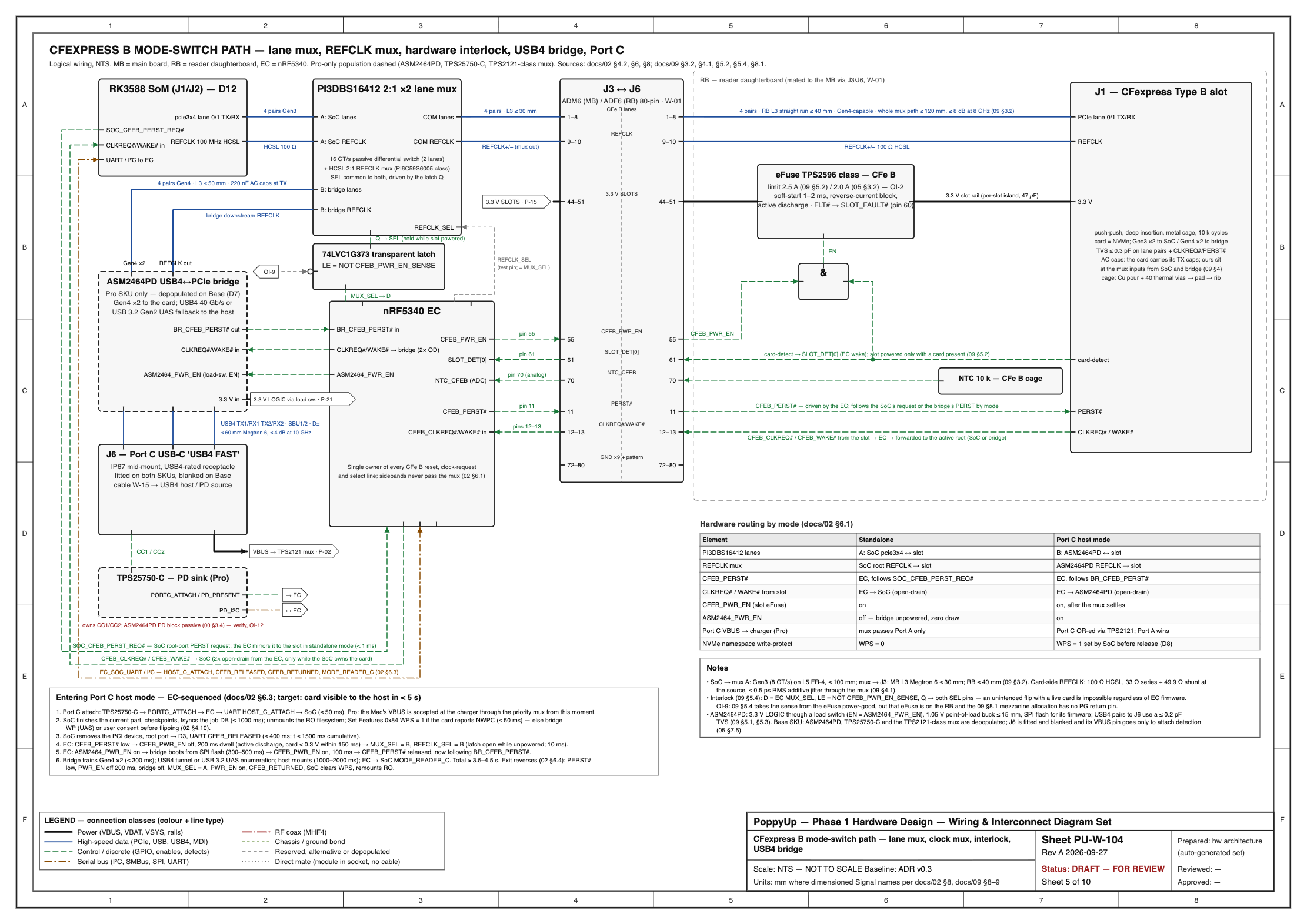
The hand-off sequence, owned entirely by the EC:
Port C PD controller detects the cable; EC tells the SoC
HOST_C_ATTACH.The job engine finishes the current part, writes a checkpoint, fsyncs the job DB, unmounts the read-only filesystem.
If the card's controller supports NVMe Namespace Write Protection, the SoC sets it (Feature 0x84, state 1) while it still owns the card.
The SoC removes the PCI device, puts the root port in D3, and tells the EC
CFEB_RELEASED(budget 1.5 s).The EC asserts the slot's PERST#, cuts slot power for 200 ms (a real controller reset), flips the lane mux and the 100 MHz reference-clock mux to the bridge side, powers the ASM2464PD (300 to 500 ms firmware boot), restores slot power, and releases PERST# under the bridge's control.
The bridge trains Gen4 ×2 to the card and brings up the USB4 tunnel or UAS enumeration; the host mounts the card.
Target: card visible to the host in under 5 seconds (the budget sums to 3.5 to 4.5 s). Detach reverses the sequence, and on return the job engine re-verifies the card by controller serial, filesystem UUID and a directory mtime scan, resumes unchanged files from their offsets, and re-queues anything the host touched.
Two hardware details make this safe rather than merely clever:
A hardware interlock. The mux select line is latched through a 74LVC1G373 D-latch that only passes a new value while slot power is off. The mux physically cannot flip under a live card, regardless of EC firmware state.
Separate connectors. The obvious "one USB-C for everything" design was evaluated and rejected. It would need a 2:1 mux on 20 GBd USB4 lanes (every sourceable part was rated to 16 GT/s, and the insertion loss lands at the connector where the budget is tightest), and it would create a PD-ownership race between the bridge, the PD controller and the SoC that behaves differently on Apple, Intel and AMD hosts. Giving the bridge its own port makes Port C a textbook ASM2464PD reference design, identical to shipping USB4 CFexpress readers, and moves the only mux to the PCIe side where 16 GT/s is exactly what the PI3DBS16412 is rated for.
3.6 The read-only guarantee on Port C#
On Port A, read-only is trivial: the SoC owns the LUNs and sets the write-protect bit. On Port C the SoC is out of the data path once the mux flips; a USB4 host talks NVMe directly to the card. Read-only therefore has to be arranged before the hand-off, and no single mechanism covers every host and card combination. The package documents a layered approach, in order of preference:
| # | Mechanism | Works for | Limits |
|---|---|---|---|
| 1 | NVMe Namespace Write Protection (NVMe 1.4 Feature 0x84, state 1) set by the SoC before the flip | Native USB4 hosts and UAS-fallback hosts alike; the host mounts the volume read-only and macOS cannot create its hidden files | Only on cards whose controller reports NWPC support (Identify Controller byte 531), expected to be a minority of camera cards. State 1 persists across power cycles, so the SoC must clear it on return, and a card pulled mid-session leaves write-protected until re-inserted |
| 2 | ASM2464PD bridge write-protect (SCSI write-protect / firmware read-only configuration) | USB 3.2 Gen2 hosts in UAS fallback (iPhone Pro, TB3-less PCs) | No effect in native USB4 mode; availability of the configuration is unverified with ASMedia |
| 3 | Explicit per-session consent | Everything else (native USB4 host plus a non-NWPC card) | Read-only cannot be enforced. The device does not switch automatically. The OLED and app ask "Mac wants write access to CFe B allow?"; the session is logged; a full re-verification runs on return |
Whether mechanism 1 covers a useful fraction of the card library, and whether mechanism 2 exists at all, are two of the first questions the proof-of-concept stage answers. Until then the consent fallback is the design assumption, and it is tracked as the second-highest risk in the register.
3.7 Tethered uplink on Port B#
There is no built-in modem. Away from infrastructure the device uploads through the user's phone (a Wi-Fi hotspot, or USB tethering on Port B) or an off-the-shelf USB LTE/5G adapter on Port B. Electrically nothing is added: the phone or adapter enumerates on the ASM3142 host controller as a USB network-class device, using ipheth for iPhone Personal Hotspot, cdc_ncm or rndis_host for Android, and cdc_mbim or qmi_wwan for cellular adapters. To the job engine it is one more network interface, tagged metered by default, with the same per-link caps, data-cap warnings and adaptive chunk size as a hotspot.
Port B sources 5 V at a user-set 0.5, 1.5 (default) or 3 A so the phone charges rather than drains. The EC permits 3 A only while PoppyUp itself has an external PD contract of at least 45 W; on battery the cap is 1.5 A regardless of the setting, so the 3 A case is never a battery-runtime case. Port B is a single receptacle: SSD ingest and tethering are mutually exclusive and the OLED says which role is active.
3.8 Networking and link policy#
Ethernet: RTL8126 5GBASE-T with NBASE-T auto-negotiation down to 2.5G, 1G and 100M. 10GBASE-T was rejected: a 10GbE PHY adds 2 to 4 W in a sealed passive enclosure whose whole ceiling is about 10 W, S3 with SHA-256 at 1.1 GB/s would consume the entire A76 cluster, and real venue uplinks rarely exceed 1 Gb/s. 5GbE is already 5 to 50× headroom over them. This decision is final in the package; no 10GbE footprint option is carried.
Wi-Fi: MediaTek MT7925 on an M.2 Key-E 2230 module, Wi-Fi 7 2×2 at 160 MHz across 2.4, 5 and 6 GHz, station and access point concurrent on the same channel. Two tri-band flex antennas sit in the front frame's upper band either side of the OLED, 118 mm apart, behind polycarbonate windows.
BLE: 5.4, on the EC rather than the Wi-Fi module, so the phone app can provision, wake and query the device while the SoC and Wi-Fi are asleep. One chip antenna at the bottom-left of the main board behind a small PC window.
Policy: Ethernet > Wi-Fi STA > USB tether by default, fully user-configurable. Automatic failover within 10 s when the standby link is already up, fail-back at the next chunk boundary. Per-link rules: never upload over metered links, caps per job or per billing period, bandwidth caps, time windows. Multi-link bonding is a firmware-phase option the hardware does not preclude, because all three links are independent interfaces.
3.9 Power#
The pack is four 21700 cells (Samsung INR21700-50E, LG M50LT or Molicel P45B class) in 2S2P: 7.2 V nominal, 10 Ah, 72 Wh, under the 100 Wh airline carry-on limit. The pack PCB carries a TI BQ40Z50-R2 gauge and protector with Impedance Track for state-of-health and runtime estimates, a BQ294xx secondary protector, a fuse and thermistors. It is service-replaceable behind a screw-down door in the front frame, which matters for the EU Battery Regulation 2023/1542 from February 2027.
The charger is a TI BQ25792 buck-boost NVDC charger fed from a TPS25750 PD controller on Port A (5 to 20 V, up to 65 W, 100 W tolerated). NVDC means the system rail is always powered from whichever source is available and the transition on PD unplug is seamless; the battery is the hold-up, which is why there is no supercapacitor. On the Pro model a third TPS25750 and a TPS2121-class priority power mux OR Port C's VBUS into the charger input with Port A taking priority, break-before-make, so a Mac (typically 15 W) powers the device through a long reader session.
Rails: a 5.0 V / 6 A system rail for the SoM, Port A source and OLED; a dedicated 5.0 V / 3 A buck for Port B through its eFuse (a single 6 A rail would see a 6.1 A coincident peak and couple phone charge-current steps into the SoM rail); 3.3 V / 4 A for the card slots with per-slot eFuses; 3.3 V / 4 A for logic; local 1.05, 1.2 and 1.8 V; and an always-on 3.3 V LDO for the EC at about 50 mW.
Realistic coincident peak draw is about 28 W for milliseconds (SoM 8 W plus a CFexpress B card at 5 W plus Port B at 15 W), about 5 A from the pack. Graceful shutdown begins at 5 % state of charge: finish or abandon in-flight chunks, flush the job DB, unmount cleanly, power-gate the slots, notify the app, then power down the SoC. The EC forces off at 3 %; cell under-voltage lockout is 2.8 V.
Runtime on a new pack at 25 °C, using 65 Wh of the 72 Wh and an 88 % conversion efficiency:
| Mode | Loads (W) | Battery draw (W) | Runtime (h) |
|---|---|---|---|
| Ethernet upload, 5GbE, CFexpress B at ~500 MB/s | 13.1 | 14.9 | 4.4 |
| Ethernet upload, 1GbE venue (~110 MB/s) | 9.2 | 10.5 | 6.2 |
| Wi-Fi upload (~80 MB/s) | 8.9 | 10.1 | 6.5 |
| Upload via phone hotspot (~10 MB/s) | 6.9 | 7.8 | 8.3 |
| Upload via USB-tethered phone, phone charged at 1.5 A | 14.1 | 16.0 | 4.1 |
| Host mode, USB4 path to Mac (Pro) | 9.0 | 10.2 | 6.4 (indefinite with the Mac powering Port C) |
| Host mode, gadget path to iPhone | 7.7 | 8.7 | 7.5 |
| Idle awake, Wi-Fi associated, OLED on | 3.3 | 3.75 | 17 |
| Standby, SoC off, EC and BLE advertising | 0.09 | 0.1 | ~600 (about 3 weeks) |
3.10 Thermal: a sealed box with a 10 W budget#
The enclosure is sealed to IP54 and has no fan. Its passive ceiling with the magnesium chassis, on a desk in free air, is about 10.0 W at 25 °C ambient and 5.7 W at 35 °C with the shutter closed, and about 9.5 / 5.4 W with the shutter parked open over the rear face. These are model values (surface area about 0.056 m², combined convection and radiation coefficient about 9 W/m²·K, ribs, a 0.80 spreading-uniformity factor for AZ91D) to be verified at EVT.
The design rests on five legs:
Conduct every watt into the chassis. The main board's component side faces the rear magnesium skin. Every part over 0.5 W gets a gap pad to a cast boss whose face is machined to 0.10 mm flatness after casting. The SoM gets a 2.0 mm, 3 W/m·K pad; the switch and PHY get 1.5 mm pads.
Use thermal mass for bursts. The effective transient heat capacity is about 500 J/K. A 5GbE upload dissipates about 14.9 W, which exceeds the ceiling at any ambient, but one 512 GB card takes about 15 to 17 minutes and the model shows the skin reaching about 45 °C from 25 °C ambient at the end of the card, below the 48 °C cap. Time to the cap is about 17 minutes from 25 °C and about 9 minutes from 35 °C. Cool-down time constant is about 19 minutes.
Throttle predictably. A ladder with 3 K hysteresis and 60 s minimum dwell: skin ≥ 42 °C derates charging; ≥ 45 °C warns and pre-caps new Ethernet links to 2.5G; ≥ 48 °C renegotiates Ethernet to 2.5G, duty-cycles Wi-Fi uploads 60 s on / 20 s off and caps card reads at 800 MB/s; ≥ 50 °C pauses card reads and stops charging. Component limits (SoC 85 °C DVFS, card SMART 70 °C pause, battery 45 °C stop charge) run in parallel.
A thermal safety rule for the device that gets packed away mid-job. The operating assumption is a desk or table; a bag is for transport only. If skin reaches 52 °C, internal air 60 °C or battery 55 °C, the EC asks the job engine to checkpoint every job, the SoC unmounts and powers down slots and radios, and the device drops to standby with "Too hot, paused, will resume" on the OLED and a BLE notification to the app. It resumes by itself when skin is at or below 42 °C and air at or below 45 °C, provided the link and cards are still present. A mechanical thermal switch remains as the firmware-independent backstop.
Reserve a fan envelope and decide on data. A 25 × 25 × 10 mm zone in the bottom band is kept clear for a sealed through-tunnel fan of the kind rugged laptops use (adding 4 to 6 W of dissipation for about 1 W, 35 g and $6 to 9). It is not designed in for EVT. The EVT-exit gate decides, on measured magnesium data corrected to production alloy, against four pass criteria. The model predicts that the 5GbE burst and hotspot uploads pass, and that Wi-Fi at 80 MB/s and USB4 reader mode are marginal, sitting right at 48 °C on a 25 °C desk.
The light matte grey finish is thermal, not cosmetic: emissivity in the thermal infrared is about 0.9 for any organic coating, but solar absorptance drops from about 0.9 (black) to about 0.4, which outdoors is the difference between about 15 W and 6 to 7 W of sun load on the rear face. Bare conversion-coated magnesium would have an emissivity of only 0.2 to 0.3 and lose the radiation half of the budget.
3.11 Mechanical: chassis, shutter, drop and ingress#
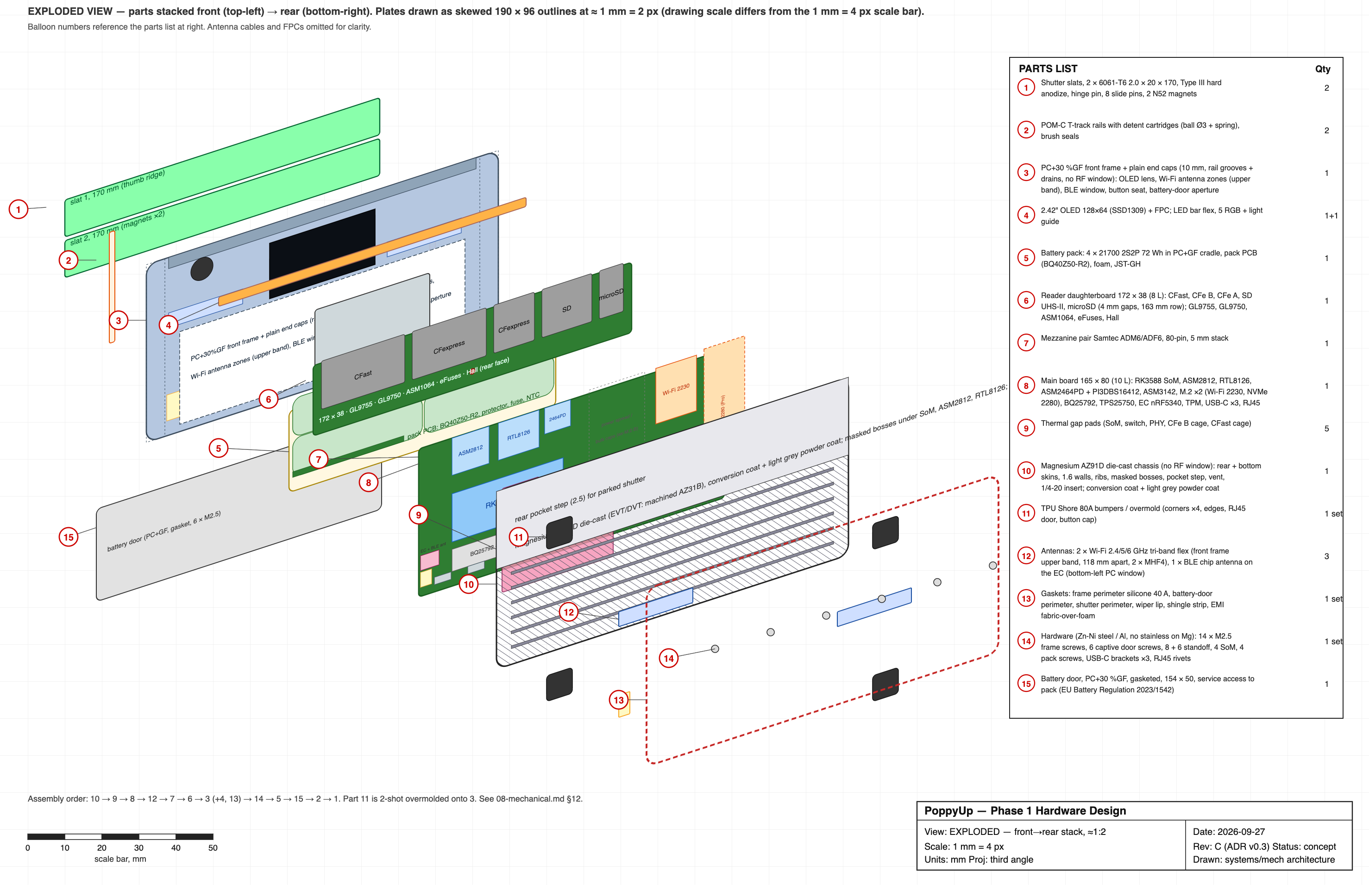
Architecture. An internal magnesium chassis-heatsink forms the rear and bottom skins and carries every connector load; a PC + 30 % glass-fibre front frame carries the RF window band, the lens and the battery door; TPU Shore 80A bumpers over mold every corner and edge. The 38 mm thickness is set by a 21 mm cell stacked in front of the main board plus a uniform 6.5 mm rear-face component budget. I decided to keep 38 mm rather than redraw for 36 mm; the 2 mm of slack goes to a taller SoM boss and thicker gap pads.
Why magnesium. AZ91D hot-chamber die-cast at 1.6 mm walls brings the device in at about 828 g against an 850 g target, where aluminum would have been about 935 g. The cost is a lower thermal conductivity (about 72 vs 96 W/m·K), hence the 0.80 uniformity factor, and a galvanic problem: magnesium is anodic to every other metal in the assembly. The package specifies a chromate-free conversion coat over the whole casting plus a 40 to 60 µm powder or e-coat outside, masked bare-conversion pads under the thermal bosses and EMI gasket lands, zinc-nickel-plated steel or aluminum fasteners with aluminum washers, aluminum or Zn-Ni inserts (no tapped magnesium, no stainless helicoils), stainless detent balls housed in POM, and anodized aluminum shutter slats that never touch the chassis. A 500-hour salt-fog coupon programme at EVT checks it. There is also an important prototype caveat: machined AZ31B prototypes conduct about 30 % better than production AZ91D castings, so EVT thermal data must be corrected (or DVT must use thixomolded AZ91D) before the fan gate is called.
The shutter. A single rigid plate wide enough to cover the top face has nowhere to go when it slides: along the length needs 163 mm of travel, rearward leaves it cantilevered 38 mm behind the device, and it cannot turn a corner into a pocket. The design is a two-slat articulated slider: two 2.0 mm hard-anodized 6061 slats, each 20 × 170 mm, joined by a full-length stainless hinge pin, running on eight pins in POM T-tracks moulded into the end caps. The track runs flat along the top, turns an R14 quarter circle at the top-rear edge, and continues 40 mm down the rear face. Travel is 36 mm. Ball-spring detents hold it at open and closed with 8 to 12 N break-out force; two N52 magnets and a Hall sensor give a clean closed signal that firmware treats as the IP54 state. A perimeter compression gasket, a silicone "shingle" over the slat joint, a wiper lip and brush seals at the rail entries provide the sealing; all channels are open-ended and the rail can be flushed with tap water. Life target: 10,000 cycles.
Drop. MIL-STD-810H Method 516.8 Procedure IV, 1.22 m onto concrete, 26 drops per sample across faces, edges and corners, five samples in DVT. Features: 7 mm TPU corner bumpers over an R8 chassis corner (estimated peak deceleration 250 to 350 g); a floating battery cradle in closed-cell foam with a 40 mm service loop; boards on standoffs with PORON washers; every external connector shell screwed or riveted to the chassis so cables never load the solder joints; captive shutter slats with hard end stops and a deeper closed detent rated for 20 N. Note that results on ductile machined AZ31B do not transfer to die-cast AZ91D, so DVT drop units must be soft-tool AZ91D shots and a repeat on production castings is a mandatory PVT launch gate.
Ingress. IP54 with the shutter closed: a moulded silicone gasket around the frame-to-chassis perimeter under 14 screws, a second gasket around the battery door, the shutter seals, IP67-rated mid-mount USB-C receptacles with integrated O-rings, a hinged TPU door over the RJ45, a sealed button, a membrane over the reset pinhole, and a Gore-type vent membrane for pressure equalisation. The enclosure penetrations are exactly those; the SIM tray from an earlier revision is gone.
3.12 The embedded controller, display and security#
The nRF5340 is the "brain stem." It is the only thing always on, has the only BLE radio, and owns every signal that must be right even when the SoC is off, hung or booting: power sequencing, the button, the fuel gauge and charger, six thermistors and the throttle requests, the PCIe mux and reset sequencing, the LED bar, the OLED (so the display works with the SoC off), the Hall sensor, card-detect wake, the RTC, the SoC watchdog and hard reset, and the thermal safety rule. It talks to the SoC over a 1 Mbaud CRC-framed UART plus I²C, and hosts a BLE "Job Location" characteristic the phone app writes so a job's manifest can carry latitude, longitude, altitude, accuracy, timestamp and source without an on-device GNSS receiver.
The display is a 2.42" 128 × 64 monochrome SSD1309 OLED driven by the EC over SPI. The package explains why not e-paper (0 °C operating floor, slow refresh, fragile glass) or memory LCD (poor readability in dark sets). Line 1 shows the mode ("UPLOADING ETH 5GbE", "READER iPhone (RO)", "TOO HOT paused, will resume"); lines 2 to 4 show per-slot progress. A 5-segment RGB LED bar along the front top edge gives per-slot state visible with the shutter closed: blue for reader mode, pulsing green uploading, solid green verified, amber paused, red error, with pulse rates that differ per state for colour-blind users.
Security: an Infineon OPTIGA SLB9672 TPM 2.0 on the SoC's SPI bus seals the LUKS2 data-partition key to boot state and holds a non-exportable ECC P-256 device identity key for mutual TLS to the app and OTA server. The RK3588 boot chain is OTP-fused root of trust → signed SPL/TF-A/OP-TEE → FIT-verified U-Boot and kernel → dm-verity root with A/B slots → LUKS2 data. The EC runs MCUboot with signed images. Endpoint credentials and OAuth tokens live only in the encrypted partition, never on the host-visible LUNs, never in logs. Debug ports are fused off at PVT.
Part 4: How it is configured#
4.1 From the user's side#
First pairing. Over BLE, with a 6-digit code on the OLED as out-of-band confirmation, establishing device-bound TLS credentials rooted in the TPM. Target under 30 seconds. BLE works with the SoC asleep, so a device in standby in a bag can be set up from the phone.
Endpoint profiles. Name, type (SFTP with password or key auth; S3 and S3-compatible in path or virtual-host style with SigV4; Google Drive with OAuth 2.0 and resumable uploads; Dropbox with upload sessions), host or bucket or folder, and credentials, synced from the app and stored only in the TPM-sealed partition. Each of the five slots has a default endpoint; per-card overrides by card serial or volume label are supported, so two cards in two slots can upload to two different services at once.
Link policy. Order of preference (default Ethernet > Wi-Fi > USB tether), per-link metered or unmetered tagging (hotspots, tethers and USB cellular adapters default to metered), "never upload over metered", per-job and per-billing-period caps with 80 % and 95 % warnings, bandwidth caps and time-of-day windows. Changes take effect at the next chunk boundary.
Wi-Fi. WPA2/WPA3-Personal and Enterprise (EAP-TLS, PEAP), captive-portal detection with app-assisted login, 6 GHz where regulation allows. The device's own access point can run concurrently with the station link for management.
Host mode. Read-only on both ports by default. A per-session read-write toggle in the app, never persisted, reverting on detach, logged. On Port A, uploads pause by default; concurrent read-only sharing is an opt-in. On Port C, a consent prompt appears only when neither write-protect mechanism applies to the attached host and card.
Port B charge current. 0.5, 1.5 (default) or 3 A; 3 A is honoured only while an external PD source of at least 45 W is attached. The app and OLED show the effective limit.
Telemetry. Per-slot job status, progress and throughput; active link and tethered-link type; metered data used against cap; Wi-Fi RSSI and SSID; battery percentage, Wh, health, cycle count and runtime estimate; temperatures and throttle or pause state; history of at least 500 jobs. Refresh under 1 s over Wi-Fi or USB, under 5 s over BLE.
Updates. Signed A/B OTA (RAUC-class) for both the SoC and EC firmware, delivered through the app or direct download, with automatic rollback on boot failure and anti-rollback counters.
Controls. One sealed button: short press wakes the display, 3 s long press is a graceful power-off, 12 s is an EC hard reset. Card insertion, a Port A or C attach, or the thermal auto-resume condition wakes the device from standby. One recessed reset pinhole. That is all.
4.2 From the engineer's side (what firmware bring-up has to configure)#
The architecture document hands these items to the firmware phase as consequences of the hardware choices:
Device tree.
pcie3x4in ×2 mode withpcie3x2enabled (bifurcation per the Rockchip TRM; verify on the chosen carrier's bootloader). The CFexpress B root port needs hot-plug behaviour; the plan is a userspace remove/rescan driven by EC events because it is deterministic.PERST# ownership. The SoC's reset GPIO for the CFexpress B port routes to the EC, not the slot; the EC mirrors it in standalone mode with under 1 ms latency and hands it to the bridge in Port C mode.
Gadget. dwc3 OTG1 fixed as peripheral. Composite via configfs:
f_tcm(UAS) plusf_mass_storage(BOT fallback) plusf_ncm, all LUNsro=1. Measure iOS behaviour with UAS early; ship BOT for iOS host IDs if needed.Drivers.
r8169for the RTL8126 (mainline from 6.9),mt7925efor Wi-Fi with the module's Bluetooth held in reset,sdhci-pci-glifor the SD controllers (UHS-II needs the 6.x UHS-II core),ahcifor the ASM1064,tpm_tis_spifor the TPM with a PCR-sealed LUKS2 key viasystemd-cryptenroll;ipheth,cdc_ncm,rndis_host,cdc_mbimandqmi_wwanfor tethering, with ModemManager started only when an MBIM/QMI adapter is present so it never touches a phone.Port C read-only flow. At every CFexpress B mount, read Identify Controller byte 531 and cache per card serial; on attach with an NWPC card,
nvme set-feature -f 0x84 -v 1before the mux flips; on return,-v 0before remounting and before "Safe to remove".XQD detection. A non-NVMe PCIe class code enumerating in the CFexpress B slot powers the slot down and shows the message.
EC protocol. Versioned, CRC-framed UART; both sides tolerate the other rebooting; a 2 s heartbeat watchdog; the EC completes a Port C hand-off autonomously if the SoC hangs mid-sequence, then hard-resets it.
Thermal. Kernel thermal zones for the SoC; the EC supplies skin, chassis, air and card temperatures over I²C; the job engine implements the throttle ladder, honours
THERMAL_PAUSE_REQand resumes onTHERMAL_RESUME.
4.3 SKU configuration#
| Base | Pro | |
|---|---|---|
| All five slots, 5GbE, Wi-Fi 7, BLE, tethered uplink | ✓ | ✓ |
| Port C USB4 CFexpress B pass-through (ASM2464PD), read-only by default | depopulated, receptacle blanked | ✓ |
| Port C PD sink (Mac powers the device in reader mode) | depopulated | ✓ |
| Internal NVMe (M.2 2280) | socket present, empty | ✓ 1 TB |
| Battery | 72 Wh | 72 Wh |
Same PCBs, same enclosure; the SKUs differ only by population. Crucially, Base is validated and shippable without Port C: firmware keeps the Port C path behind a feature flag, the Base functional-test fixture does not exercise Port C, and Base regulatory testing covers the Base population. The Pro USB4 population gets its own FCC Part 15B declaration addendum, a RED technical-file update and a 62368-1 variation (estimated $8 to 15k) later. A slip on any Port C item moves the Pro date, never the Base date.
Part 5: The honest numbers#
All rates decimal (1 MB/s = 10⁶ B/s), "realistic" meaning what a well-implemented stack achieves in the field.
Where the bytes actually slow down#
| Path | Realistic rate | What limits it |
|---|---|---|
| CFexpress B 4.0 card inside PoppyUp | ~1.65 GB/s | RK3588 root port negotiates Gen3 ×2 (the card is capable of 3.5 GB/s) |
| CFexpress A 4.0 inside PoppyUp | ~850 MB/s | Gen3 ×1 switch port |
| SD UHS-II | 280 to 300 MB/s | Card |
| CFast 2.0 | 480 to 550 MB/s | Card and the ASM1064's AHCI engine |
| microSD UHS-I | 90 to 100 MB/s | Bus |
| External SSD on Port B | ~900 MB/s | SSD |
| 5GBASE-T to S3 | 480 to 520 MB/s | TCP ramp per part, TLS, server pacing |
| 2.5GBASE-T / 1000BASE-T | 270 to 290 / 105 to 115 MB/s | Link |
| Wi-Fi 7, 6 GHz, 160 MHz, 3 m line of sight | 200 to 280 MB/s | Airtime |
| Typical venue Wi-Fi, 80 MHz at 10 m | 75 to 110 MB/s | Contention |
| Phone's 5G uplink, good C-band cell | 12 to 25 MB/s | Cell uplink scheduling |
| Phone's 5G uplink, typical | 2.5 to 10 MB/s | Operator uplink allocation, 23 dBm phone power |
| Phone's LTE, rural | 0.25 to 2 MB/s | Path loss |
| Host via Port C, USB4 Mac (Pro) | 2.8 to 3.2 GB/s | Card and tunnel tie |
| Host via Port C, iPhone Pro (Pro) | 900 to 1,000 MB/s | USB 3.2 Gen2 |
| Host via Port A, any USB 3 host | 380 to 420 MB/s | 5 Gbps gadget |
| Host via either port, USB 2.0 iPhone | 35 to 40 MB/s | The phone |
Time to move a card#
| Path | Rate | 256 GB | 1 TB |
|---|---|---|---|
| Quick copy CFexpress B → internal NVMe (Pro) | 1,500 MB/s | 2.8 min | 11 min |
| Host, USB4 Mac (Pro) | 3,000 MB/s | 1.4 min | 5.6 min |
| Host, iPhone Pro (Pro) | 950 MB/s | 4.5 min | 18 min |
| Host, Port A gadget (any SKU) | 400 MB/s | 11 min | 42 min |
| Host, USB 2.0 iPhone | 38 MB/s | 1.9 h | 7.3 h |
| Upload, 5GBASE-T to S3 (studio) | 500 MB/s | 8.5 min | 33 min |
| Upload, 1000BASE-T | 110 MB/s | 39 min | 2.5 h |
| Upload, typical venue Wi-Fi | 90 MB/s | 47 min | 3.1 h |
| Upload, 100 Mb/s venue uplink | 11 MB/s | 6.5 h | 25 h |
| Upload via phone on 5G, good cell | 18 MB/s | 4.0 h | 15.4 h |
| Upload via phone on 5G, typical | 6 MB/s | 11.9 h | 46 h |
| Upload via phone on rural LTE | 1 MB/s | 71 h | 12 days |
The ratio between the internal read rate and a typical phone uplink is about 275×. Over a phone, PoppyUp is a background uploader that runs for hours on a cart or desk; the firmware must let the user prioritise selects, proxies and stills before RAW. Over studio Ethernet it is a foreground tool that finishes a card in minutes. No hardware, including a built-in modem, changes the cellular rows.
Part 6: What it costs#
Bill of materials#
Budgetary costs in USD, mid-2026, including PCBA and box-build labour, excluding tooling, NRE, certification, software, warranty, freight and duty. Confidence: ±15 % on silicon, ±25 % on mechanical, ±30 % on assembly.
| Group | Base @1k | Base @10k | Pro @1k | Pro @10k |
|---|---|---|---|---|
| Compute (SoM, carried at Firefly Core-3588J pricing as a placeholder) | $99 | $81 | $99 | $81 |
| PCIe fabric and bridges | $21 | $16 | $39 | $29 |
| Card slots and controllers | $18 | $14 | $18 | $14 |
| Networking | $10 | $8 | $10 | $8 |
| Wi-Fi / BLE | $18 | $12 | $18 | $12 |
| EC / UI | $18 | $13 | $18 | $13 |
| Security | $2 | $2 | $2 | $2 |
| Power | $68 | $52 | $72 | $55 |
| Connectors | $40 | $30 | $40 | $30 |
| PCBs | $41 | $22 | $41 | $22 |
| Mechanical | $93 | $42 | $155 | $94 |
| Assembly and test | $53 | $30 | $56 | $32 |
| Packaging and accessories | $8 | $6 | $8 | $6 |
| Total | $488 | $327 | $575 | $397 |
The SoM is about 20 % of the Base BOM and the single biggest lever; board-down RK3588J would save $25 to 35 per unit for about $120k of NRE and is one of the three paths in the proof-of-concept bake-off. The magnesium chassis is $58 at 1k (machined or thixomolded) falling to $21 at 10k (die-cast). The Pro adder is about $18 of USB4 bridge path, $3.80 of Port C power parts, $62 of NVMe and $3 of extra test.
One-time costs#
| Item | Estimate |
|---|---|
| Tooling and fixtures (Mg die-cast tool $62k, PC frame mould $40k, TPU overmold $28k, shutter dies and POM moulds $18k, gaskets $12k, lens $6k, pack holder $8k, test fixtures $22k) | ~$196k |
| Magnesium thixomold / soft tool for DVT thermal units (prototype tooling, in the DVT budget) | ~$35k (verify) |
| Certification for the Base launch (FCC incl. Wi-Fi SAR, ISED, CE RED incl. EN 18031, UKCA, UN 38.3, IEC 62133-2, UL 62368-1, MIL-STD/IP lab, memberships, one re-test cycle) | $160 to 295k; realistic planning figure ~$190k |
| Pro population regulatory addendum, after Base launch | $8 to 15k (verify) |
The whole program#
| Block | US fully-loaded staffing | ODM-supported / lower-cost |
|---|---|---|
| Hardware program to mass production (PoC, EVT, DVT, PVT units, tooling, certification) | $1.1 to 1.4M | $1.1 to 1.4M |
| Phase 1 engineering staffing through MP (about 120 vs 90 person-months) | $2.2 to 2.6M | $0.9 to 1.3M |
| Phase 2 firmware (job engine, connectors, EC, OTA, security) | $0.5 to 0.9M | $0.25 to 0.45M |
| Phase 3 apps (iPhone first, then desktop) | $0.4 to 0.6M | $0.2 to 0.3M |
| Contingency 20 to 25 % | $0.9 to 1.3M | $0.5 to 0.8M |
| Total | ≈ $5.5 to 6.5M | ≈ $3.2 to 3.9M |
Ranges are deliberately wide. A target retail price and a budget ceiling were never set, so the package stops short of a gap analysis; the levers it names are volume, SKU mix, ODM rates and scope, and deferring the Pro track.
Part 7: The decision that shaped the product: no built-in modem#
The first revision of this design (v0.1) had a Quectel RM520N-GL 5G modem in an M.2 Key-B slot, a dedicated 5 A rail, a nano-SIM tray, an eUICC and four cellular antennas in the end caps. Revision v0.2 deleted all of it, and review in v0.3 made the deletion final with no reinstatement provisions. The reasoning is worth reading in full in the ADR; the short version:
The uplink was never the hardware's to fix. Real-world sub-6 GHz 5G uplink is 2.5 to 10 MB/s, 150 to 650× below the card read rate. A 256 GB card takes 7 to 28 hours over cellular. A phone hotspot delivers the same uplink from the same cell.
Cost. About $146 at 1k of BOM, the largest single line at 19 to 24 % of the Base SKU, plus $100 to 150k of one-time certification (GSMA TAC, PTCRB, GCF, carrier programs, cellular SAR) and about $40k of DVT carrier-lab entry.
Schedule. The PTCRB → carrier chain was the critical path after DVT (Verizon ODI alone is 12 to 20 weeks, serial with the FCC grant). Removing it moved mass production about a month earlier and freed launch messaging from carrier approvals.
Thermal and power. The modem was the hottest sustained source (4.5 to 6 W) and the only 12 W burst load. Its removal deleted a buck, 12 W of peak-current sizing, and put every non-Ethernet upload mode under the passive ceiling.
Mechanical. One fewer sealed penetration, four fewer antenna cables, no RF-transparency constraint on the end caps, and the tallest rear-face part gone.
Supply and firmware. A 12 to 20 week lead-time, carrier-firmware-locked, single-vendor part and the whole MHI/MBIM/eSIM firmware surface removed.
What it costs: no upload without infrastructure or a phone, and the phone's battery becomes part of the field kit (mitigated by Port B charging it while tethered). The positioning shifts from "5G built in" to "uses the cellular you already carry." The risk register keeps this as a market-perception item: reviewers may count "no modem" against the product even though the achievable uplink is identical.
Part 8: The roadmap, if you want to build it#
The package lays out a 15-month path from a program start to first shipment in five stages, with four hard gates. The documents used an illustrative calendar starting October 2026; I give the stages in relative months here because nobody has started the clock.
Timeline at a glance#
| Stage | Months | Units | Purpose | Cost |
|---|---|---|---|---|
| PoC | 0 to 2 | 3 dev-kit rigs | Retire architecture-level risks on off-the-shelf boards before any schematic; choose the SoC carrier | ~$20k |
| EVT | 3 to 7 | 15 to 20 board sets, 5 full units | First custom PCBs in a machined magnesium enclosure; prove electrical, thermal, RF and mode switching; fan gate at exit | $120 to 160k |
| DVT | 7 to 12 | 60 to 100 | Near-final tooling (Mg soft tool); drop, ingress, life, pre-compliance; formal FCC/ISED/CE submissions | $345 to 500k |
| PVT | 12 to 15 | 200 to 500 | Production tooling and line at the ODM; yield, test coverage, final certs, packaging | ~$195k tooling + $250 to 300k units |
| MP | 15+ | ramp to ~300/month | Ship Base; Pro follows when its track is done |
Gates: PoC exit (SoM vs board-down decision), ODM design review before the EVT schematic, EVT exit (fan decision on corrected magnesium data), and the standing rule that Base launch is decoupled from Port C.
Stage 1: Proof of concept (months 0 to 2)#
Three bench rigs with identical peripherals and one SoC platform each, because the carrier form is undecided: a Firefly Core-3588J, a Forlinx FET3588-C, and a board-down RK3588J on the ODM's reference board (or the Rockchip EVB). Around each: a PCIe ×4 slot → ×2 riser → PI3DBS16412 evaluation board → M.2-to-CFexpress B adapter; a bare ASM2464PD USB4 NVMe enclosure board fed from the mux's B side; a commercial ASM2812 quad-M.2 riser carrying an RTL8126 card, a GL9755 SD card, a GL9750 microSD, an ASM1064 SATA card with a CFast adapter, an ASM3142 USB host card and a WD SN770 NVMe; an MT7925 module with two antennas; an nRF5340-DK as the EC stand-in; and TI evaluation modules for the BQ25792, two TPS25750s, the TPS2121 mux and the BQ40Z50-R2 with a bench 2S2P pack. Rig cost about $4 to 5k each, plus about $3k for a representative card library and $2k for network peers.
Fifteen tests retire the architecture-level assumptions. The ones that matter most:
P1
pcie3x4bifurcates ×2 + ×2 on each platform; CFexpress B 4.0 cards from three vendors train Gen3 ×2 and read at or above 1.6 GB/s.P2 Hot re-route of the CFexpress B slot between the SoC and the bridge through the mux with scripted sequencing from the nRF5340-DK: 1,000 cycles, zero training failures, card filesystem clean.
P3 ASM2464PD to an M-series Mac at or above 2.8 GB/s and to an iPhone 15 Pro at or above 900 MB/s via UAS fallback.
P4 dwc3 UAS and BOT gadgets to Mac, Windows and both iPhone classes at or above 380 MB/s (USB 3) and 38 MB/s (USB 2), read-only enforced, composite with NCM driverless.
P5 S3 over 5GbE with TLS 1.3, SHA-256 and xxHash64 at or above 480 MB/s on at most two A76 cores.
P7 USB tethering: iPhones and Android phones enumerate within 10 s after the trust prompt, uplink at or above 90 % of the phone's own speed test at five sites, 100 attach/detach cycles, Port B current control verified and 3 A refused without a PD source.
P13 The NWPC survey: read Identify Controller byte 531 on every card in the library and confirm whether namespace write protection is accepted and survives the slot power cycle.
P14 The ASM2464PD read-only configuration check with ASMedia.
P15 The SoM / board-down bake-off, scored 0 to 3 on seven weighted criteria: bifurcation and lane exposure, both USB3 OTG with working gadget, thermal interface, longevity terms in writing, price, second-source story, and the ODM's ability to support the path.
Exit: P1 to P5 pass; P6 to P14 pass or have an approved fallback; the carrier decision is made; an updated ADR v0.4 carries measured numbers; the ODM design-review package goes out. Two engineers for two months plus a part-time firmware engineer.
Stage 2: Engineering validation (months 3 to 7)#
Before the EVT schematic starts, the ODM receives a design-review package (ADR, block diagram, component selection, PCB architecture, mechanical concept, BOM, PoC report) and a question list: preferred parts, DFM/DFT feedback on the 10-layer hybrid stackup and the 0.635 mm mezzanine, test capability, magnesium die-cast and coating suppliers, a battery-pack vendor, whether they have an RK3588 board-down reference design, and tooling ownership and escrow terms. The review is a gate, not a courtesy.
What gets built: the 10-layer hybrid main board (Megtron 6 or I-Speed on the USB4 and Gen4 mux layers; two fab spins budgeted), the 8-layer reader board in two variants (full five-slot and no-CFast, to prove the daughterboard concept), a hand-built pack with the production-intent pack PCB, and a machined AZ31B magnesium chassis (or thixomolded AZ91D) with the production coating stack and masking, plus coated coupons for the salt-fog programme, plus an SLA PC frame stand-in and machined shutter slats on production-intent POM rails. Fifteen to twenty board sets; five fully assembled units (three Base, two Pro); four pneumatic card insert/remove cyclers.
What gets validated: eye and BER on every high-speed path with at least 20 % mask margin; 1,000 mode-switch cycles per port with live uploads; a card matrix of at least 25 cards with the NWPC flag recorded for each; host compatibility across M1 to M6 Macs, Intel and AMD USB4 PCs, iPhone 15 through 18 Pro and iPad Pro; rail transients, charge, efficiency, hot-unplug and standby power; the full thermocouple map with the shutter closed and open at 25, 35 and 45 °C, corrected for AZ31B to AZ91D conductivity; the 500-hour salt-fog coupons; antenna efficiency in the coated enclosure and a 1 TB read under maximum Wi-Fi transmit with zero errors; EMC pre-scan with 6 dB margin; and the secure-boot chain on development keys.
The EVT-exit fan gate passes only if all four hold on corrected data: (a) one 512 GB 5GbE upload completes without throttling at 25 °C and runs at least 8 minutes at 35 °C; (b) Wi-Fi at 80 MB/s and USB4 reader mode each run 60 minutes at 25 °C without throttling; (c) hotspot or tether upload runs indefinitely at 30 °C; (d) skin stays at or below 48 °C metal and 55 °C plastic throughout. Any fail designs the sealed tunnel fan into DVT. The model predicts (a) and (c) pass with one to two minutes of margin and (b) is marginal; if (b) alone fails narrowly, I may record an explicit acceptance of "throttles on a warm desk" instead, but that is a documented decision, not an assumption.
Team: two electrical engineers (the high-speed one needs Gen4/USB4 layout experience), one mechanical, a half-time RF contractor plus an antenna house, two firmware, a half-time program manager, and the ODM liaison. Firmware delivers a bring-up image, EC firmware v0 with sequencing, gauge, thermal ladder, safety rule, Port B policy, OLED and BLE provisioning, and a job-engine skeleton for S3 and SFTP.
Stage 3: Design validation (months 7 to 12)#
The product, not the board. Sixty to a hundred units with a DVT layout by the ODM, a thixomolded or T0 soft-tool AZ91D chassis (~$35k) so drop and thermal data reflect production alloy, production PC and TPU soft tools, stamped and anodized shutter slats, moulded seals, and a production-intent pack from the ODM-managed vendor with UN 38.3 and IEC 62133-2 testing started on ten packs. An LDS-on-PC antenna trial on ten units de-risks the volume cost-down. If the fan gate failed, every unit carries the sealed tunnel fan.
Validated: the 26-drop matrix on five AZ91D units with cards inserted; IP54 closed and IP52 open at an accredited lab; the climate chamber in every mode; the thermal safety rule (device wrapped and packed mid-job, must checkpoint and auto-resume with zero data loss, ten times); 500-hour salt fog on three coated castings with disassembly inspection; vibration; 10,000 shutter cycles on three units; UN 38.3 and IEC 62133-2 on the pack; runtime per mode on five units; the final thermal map on production alloy; full FCC 15B/15C, RED and Wi-Fi SAR pre-compliance at 3 dB margin followed by formal submissions on the Base population; a 62368-1 pre-assessment; and the first feature-complete firmware with all four endpoint types, all link policies, the app alpha, and ten target users in usability testing. First-pass yield at the functional tester must reach 90 %.
Exit: all P0 requirements verified on the Base population, environmental and battery reports in hand, formal submissions made, hard tooling released (ODM-owned), final BOM and quote, fewer than ten ECOs and none touching tooling. Pro-track status reported but not gating.
Stage 4: Production validation (months 12 to 15)#
Two to five hundred Base units on the ODM's line with hard tooling: production AZ91D hot-chamber castings with production coating and masking, PC+GF frame, TPU overmold, stamped shutter, production packs with the UN 38.3 certificate, LDS antennas if the trial passed, fused secure boot with production keys, and laser-marked regulatory labels. Line targets: cycle time under 6 minutes per unit, first-pass yield at or above 95 %, Cpk at or above 1.33 on shutter force, leak test and RF power. Mandatory regression on production castings: three units repeat the 26 drops, five repeat IP54, because die-cast AZ91D differs from soft-tool shots in porosity, ductility and coated parting lines. Grants confirmed against PVT units, UKCA declaration, UL 62368-1 CB report, RoHS/REACH declarations including the chromium-free coating. Debug fusing verified on every unit. ISTA 3A packaging test. Service manual, factory test spec, golden units.
Stage 5: Mass production (month 15 onward)#
Ramp to about 300 units per month; monthly ongoing reliability testing of five units plus quarterly drop and IP on castings; an ECO board; second-source qualification for the SoM if one was chosen; the Pro population as a line variant once its fixture and regulatory addendum are complete; and, past 10k units per year, a board-down cost-down study if a SoM was chosen.
Long-lead items to start early#
| Item | Lead time | Decision gate |
|---|---|---|
| Magnesium die-cast chassis tool (AZ91D, hot-chamber) | 14 to 16 weeks plus 4 weeks for T1 samples | Hard tool at DVT exit |
| Magnesium thixomold / T0 soft tool | 8 to 10 weeks | Release at EVT exit |
| Magnesium coating supplier qualification | 8 to 12 weeks including coupon salt fog | Start at EVT kick-off |
| PC+GF front frame injection tool | 10 to 12 weeks | Soft at EVT exit, hard at DVT exit |
| SoC carrier (SoM allocation 8 to 12 weeks; board-down RK3588J plus DDR 12 to 20 weeks) | Volume PO at DVT exit | |
| 21700 cells with UN 38.3 reports; pack vendor NRE 6 weeks | 8 to 12 weeks | Pack vendor at EVT |
| Deep-insertion CFexpress and SD connectors, some custom | 6 to 10 weeks; +12 weeks if a custom depth is needed | Confirm at PoC |
| ASMedia NDA and firmware tool access | Engage at PoC start |
What firmware needs from hardware at hand-off#
The roadmap closes with the seventeen artifacts Phase 2 needs, delivered in draft at EVT-B and final at DVT: schematics and netlists with population tables; the complete device tree and pinmap; the EC-to-SoC protocol specification with timing guarantees; the mode-switch sequence with exact GPIO timings; the NVMe write-protection flow and per-card results; the Port C consent UX and decision tree; the Job Location characteristic; the Port B policy; the thermal-safety state machine; the power-state table; the sensor map and throttle table; the secure-boot key hierarchy and partition plan; the factory test interface; the card and host compatibility matrix with quirks; the measured power table; tethering integration notes; and the regulatory constraints the software must enforce (per-band power tables, 6 GHz rules, SAR duty cycles).
Part 9: What is unresolved, and what I found wrong in my own package#
A design package that claims to have no open questions is lying. These are the ones the package carries forward.
Open decisions#
SoM vs board-down. Decided at PoC exit by the bake-off.
Fan. Decided at EVT exit on corrected magnesium thermal data.
Port C read-only mechanism. How many cards support namespace write protection; whether the ASM2464PD can be configured read-only in UAS mode; whether the bridge tolerates enumerating before a downstream device appears; how to handle a card pulled while write-protected; which entity owns Port C's PD lines.
Magnesium coupon and thermal-correction results. 500-hour salt fog, gasket contact resistance, the AZ31B-to-AZ91D correction factor.
Target retail price and program budget ceiling. Never set.
Top risks (exposure = likelihood × impact)#
| # | Risk | Score | Retire by |
|---|---|---|---|
| R1 | Mode-switch hot path (mux, clock mux, reset sequencing) | 12 | PoC → EVT (Pro track) |
| R2 | Port C read-only enforcement | 12 | PoC (mechanism) → DVT (UX) |
| R3 | Thermal ceiling in a sealed passive enclosure | 12 | EVT exit |
| R4 | RK3588 software maturity: UAS gadget to iOS, PCIe hot rescan, ASPM with a switch, tethering stack | 12 | PoC / EVT |
| R5 | iPhone Files app behaviour with the gadget and the bridge fallback | 12 | PoC |
| R6 | Shutter wear, grit, drop deformation, seal | 12 | EVT / DVT |
| R7 | Magnesium corrosion and galvanic coupling | 9 | EVT coupons / DVT castings |
| R8 | Magnesium thermal fidelity (prototype alloy vs production alloy) | 9 | EVT exit |
| R9 | ODM dependency (schedule, IP, reference-design quality, tooling ownership) | 9 | PoC exit / EVT |
| R10 | SoM selection, longevity, single source | 9 | PoC exit / DVT |
| R11 | High-speed signal integrity: USB4 at 20 GBd, Gen4 through a mux, Gen3 across a mezzanine | 9 | EVT |
Conflicts the derived artifact exposed#
Building the wiring set and the 3D viewer forced every rail, pin and dimension to agree across fourteen documents. They did not, in twenty-one places. The wiring set lists sixteen (OI-1 to OI-16), including: the mechanical thermal switch rated 48 °C in three documents and "60 °C class" in the ADR, with its location and interrupted circuit unspecified anywhere; slot eFuse limits that differ between the PCB and power documents; a 6-pin pack connector allocation that needs a 5 A-per-pin family when JST GH cannot deliver it; the Hall sensor placed on both the reader board and the button flex; the always-on LDO fed from VBAT in one document and VSYS in another; the mode-switch interlock latch needing a power-good signal from an eFuse on the reader board when the mezzanine has no return pin for it; the SoM connector count given as both two and three; the reader board as both 172 and 180 mm; Port C PD ownership; USB-C plug-flip handling undocumented; the reset switch with no connector or EC signal; the LED-bar supply missing from the mezzanine; and Wi-Fi coax lengths of 120 mm in one document and 140 to 150 mm in another. The 3D viewer added five more: the OLED outline overlapping the battery door aperture by 1 mm, the reader board's height intruding into the pack, the reader board's Z position versus the slot centreline, the main board's X span versus the port positions, and the Hall sensor position.
None of these breaks the architecture. All of them are exactly the kind of thing a PoC-exit ADR revision should clean up, and I list them so whoever picks this up knows where to start.
Part 10: What is in the package#
| Item | Contents |
|---|---|
docs/00-architecture-decisions.md | The single source of truth: every decision, target number, SKU definition, owner question with status, and the v0.2 and v0.3 change records |
docs/01-requirements.md | About 140 requirements across functional, performance, interface, safety, environmental, UX and regulatory categories, each with a measurable acceptance test, a priority and the stage at which it is verified |
docs/02-system-architecture.md | Block diagram and topology tree (Mermaid), subsystem narrative, mode and concurrency table, mode-switch sequence diagrams with timing budgets, failure-mode table, boot and power state machine, the EC-to-SoC signal list, firmware hand-off notes |
docs/03-datapath-bottlenecks.md | Link-by-link throughput, CPU budget, per-mode limiter, worked upload times, headroom analysis, PoC measurements |
docs/04-component-selection.md | Two to four options per subsystem, the pick and the reasoning, part numbers |
docs/05-power-budget.md | Battery chemistry and configuration trade, power tree, rail-by-rail regulator selection, per-mode ledgers, PD behaviour, charging, hold-up, standby and wake |
docs/06-thermal.md | Heat sources, enclosure model, thermal mass, conduction paths, sensors, throttle ladder, fan envelope and gate, cold, validation plan |
docs/07-rf-antenna.md | Antenna count and placement, RF windows in a metal enclosure, coexistence, SAR, validation |
docs/08-mechanical.md | Envelope, mass budget, zoning and Z-stacks, materials, magnesium DFM and galvanic rules, slot arrangement, shutter mechanism, ports, drop, sealing, thermal interfaces, serviceability, assembly sequence, CTQs |
docs/09-pcb-architecture.md | Board set, stackups, loss budgets, high-speed rules, power integrity, EMC, the 80-pin mezzanine allocation, connector tables, test, DFM, simulation deliverables |
docs/10-bom.md | Line-item BOM at 1k and 10k, Base and Pro, tooling, cost-down levers, MSRP implications, cost risks |
docs/11-certification.md | FCC, ISED, CE, UKCA, battery, safety, ruggedness verification, logo programs, cost and timeline |
docs/12-risks-open-questions.md | Ranked register with mitigations, owner decisions with status, remaining open items, assumptions |
docs/13-roadmap.md | PoC → EVT → DVT → PVT → MP with gates, tests, costs, team and the Phase 2 hand-off list |
drawings/ | Top, front, side and exploded views as SVG, regenerated from a Python script |
wiring/ | Ten A3 sheets (system interconnect, power distribution, EC control wiring, mode-switch path, mezzanine pins, battery pack, external ports, peripheral pinouts, connection schedule), generated from a single Python model, with a CSV schedule, combined PDF and validation report. Status: draft for review |
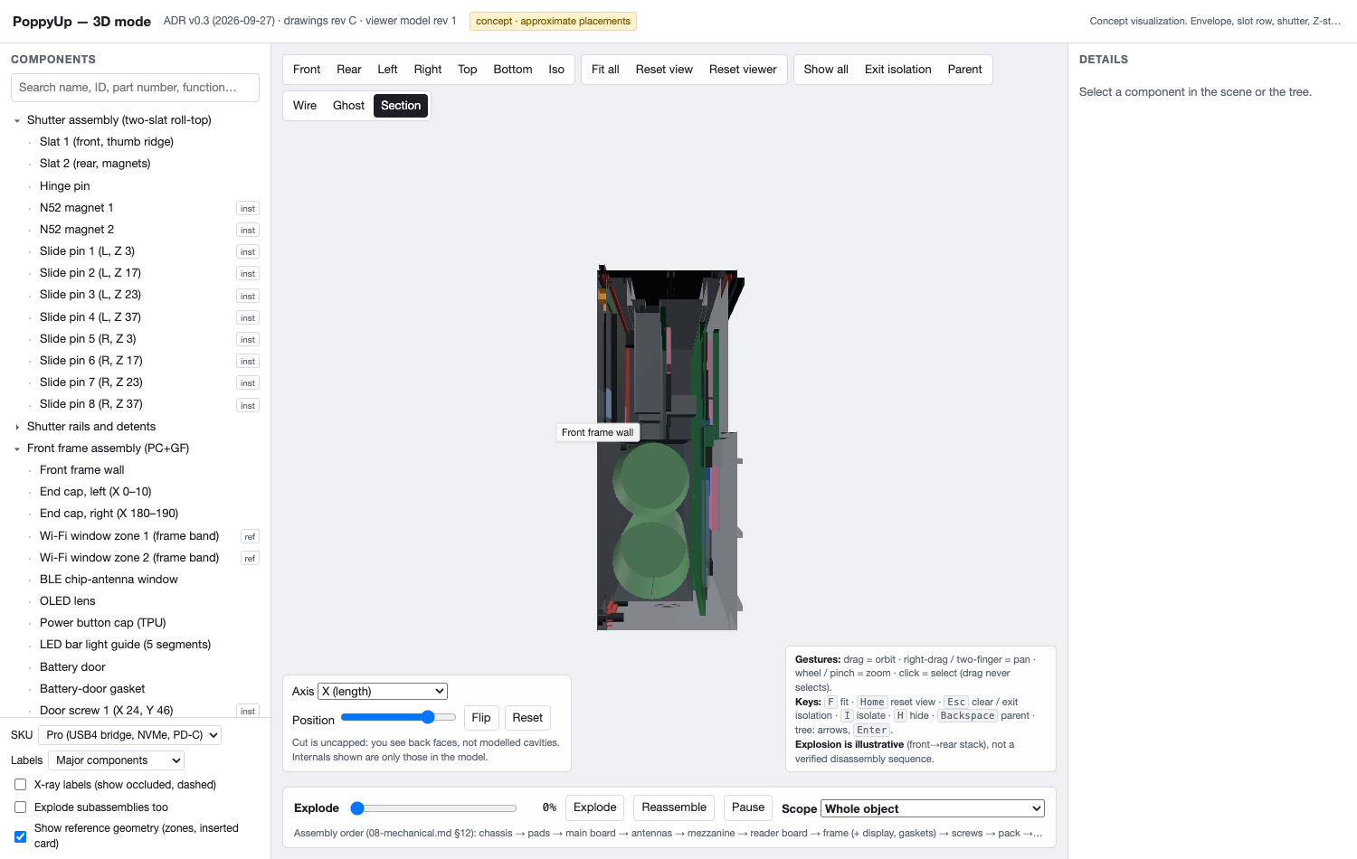
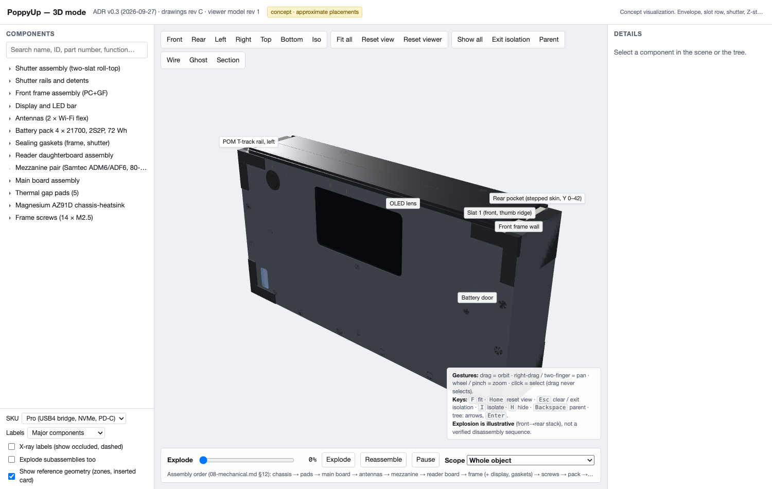
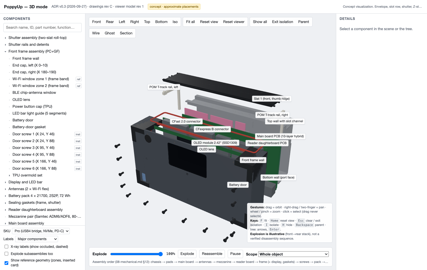
viewer/ | A browser-based three.js assembly explorer with 137 components, labels, exploded view, isolation, section plane and a Base/Pro toggle, generated from the numbers in the documents |
What is not in the package: any PCB layout, schematic capture or netlist (the wiring sheets are logical, not a schematic), any CAD model (the viewer geometry is procedural), any firmware or app code, and any measurement. Everything is paper. That is what "Phase 1" means.
License and how to use this#
I am releasing the package free of charge. Take it, fork it, build it, sell it. The only things I ask are that you keep the attribution, that you keep the "(verify)" markings honest until you have measured the thing yourself, and that you do not ship a device that writes to people's cards without telling them.
A few words of caution for anyone who does pick it up:
It is a design, not a product. Nothing has been fabricated. Every thermal, runtime and cost number is a model or a budgetary quote. The first thing the roadmap does is spend two months and $20k proving the architecture on dev kits before anyone draws a schematic. Do that.
The ASMedia parts need an NDA. The ASM2812, ASM2464PD, ASM3142 and ASM1064 have gated documentation and firmware tools. Off-the-shelf boards carry them for the PoC, but you need access for EVT. The package keeps a Broadcom PEX8724 fallback for the switch.
Magnesium is unforgiving. Read the galvanic table before you order a single fastener. Read the machining fire-safety note before you send a part to a CNC shop.
The read-only promise on Port C is the hardest problem in the product. Survey your card library first. If namespace write protection turns out to be rare, the consent prompt becomes the normal case and the product copy has to say so.
If you build it, or any part of it, I would genuinely like to hear about it.